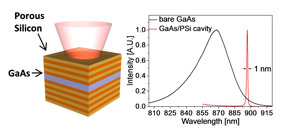
Porous Silicon (PSi) was first discovered in the mid-1950s, but it was a room temperature display of visible luminescence decades later that drew widespread attention. Efforts at all-Silicon (Si) light-emitting devices with PSi ensued. But, despite progress, performance never justified widespread implementation. While interest in PSi for Si-based optoelectronics has subsided, PSi has gained a reputation as a versatile optical material, due largely to its ability to form high-quality optical superlattices through a time-varying current density during electrochemical formation. This enables high-quality factor microcavities that could be coupled with highly efficient emitters and provide a new platform to strongly manipulate emission for applications like lasers and quantum information processing. A hybrid structure composed of a well-defined, high-quality emitting cavity layer between PSi photonic crystal mirrors is particularly attractive to bridge the gap between Si photonics and optoelectronic devices. We have shown that such PSi-based hybrid photonic architectures can be achieved with a modified transfer-printing technique.
Giang-Chau Ngo
Mapping the Brain and T2*
Beckman Institute for Advanced Science and Technology