Article
One of Beckman’s core values is to achieve excellence in science, technology, engineering, and mathematics. With the new addition of a scanning transmission electron microscope to the institute’s Microscopy Suite, innovation in STEM takes on a double meaning.
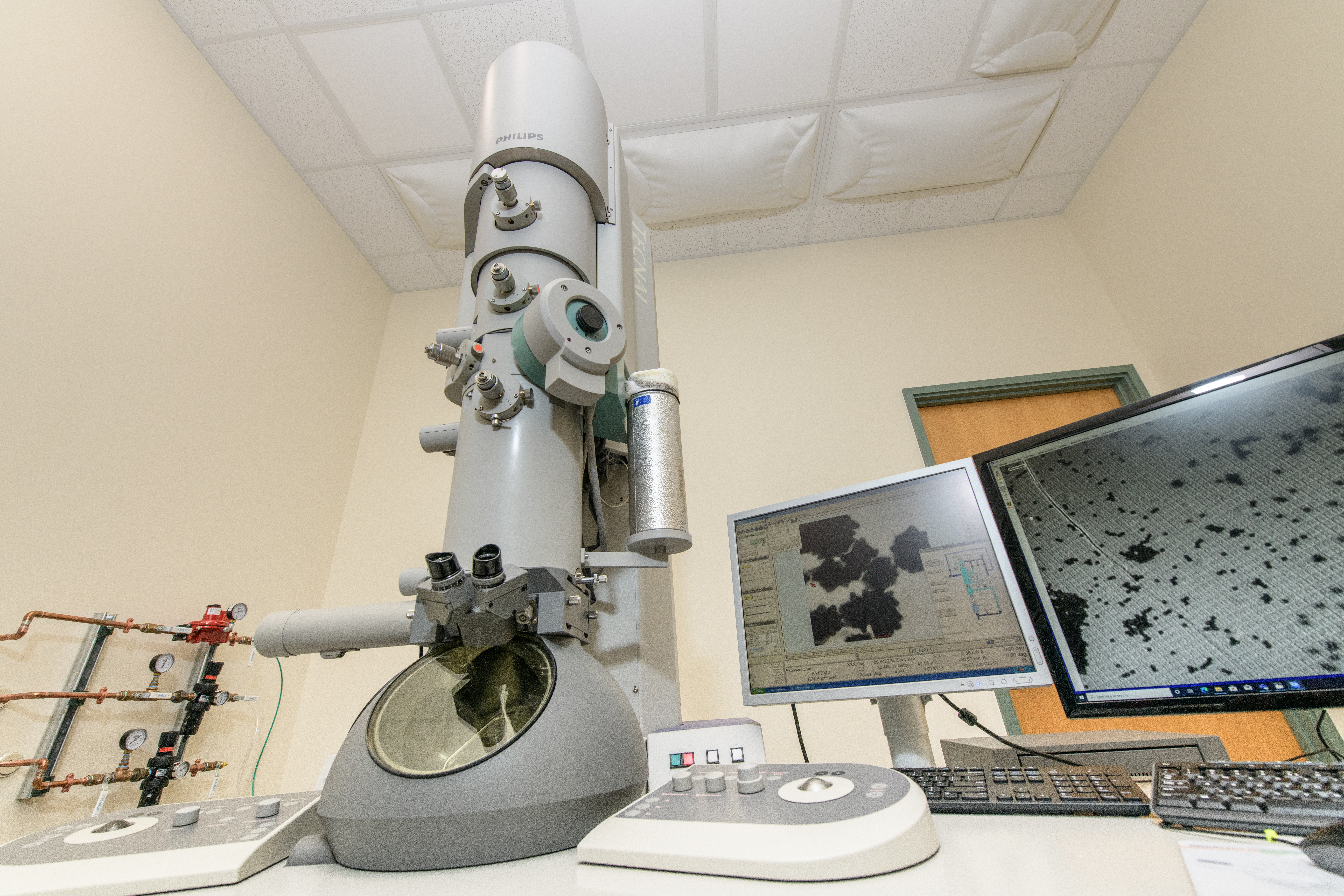
 Adding the (S)TEM to Beckman's Microscopy Suite meant that the ceiling of room B606B had to be physically raised. Tucked away in the basement of the Beckman Institute, the Microscopy Suite steadily hums with activity. Its state-of-the-art microscopes support scientists with advanced microscopy, spectroscopy, and image rendering capabilities. A recently acquired scanning
transmission electron microscope will amplify those opportunities, raising the bar for integrative imaging research at Illinois.
Not just the bar, but the ceiling. The microscope – ordered in November 2019, received in August 2020, and installed in early November that year – was so physically massive that the ceiling of room B606B had to be raised.
 Cate Wallace“It’s so exciting to add this machine to our research arsenal after our old TEM would no longer function,” said Microscopy Suite Manager Cate Wallace. “It’s great to see old users, and of course new users, coming
back to Beckman to use the (S)TEM.”
The (S)TEM is effectively the best of both microscopy worlds, capable of holistic, high resolution imaging. Each letter in the machine’s acronym highlights a unique feature.
The E marks the machine as an electron microscope, wherein a beam of electrons pass through a thin sample in the same way light passes through a conventional microscope.
The S, which stands for “scanning,” indicates features of a scanning electron microscope, which can produce a 3D rendering of a solid specimen by rasterizing an electron beam across its surface. Imagine scanning a flashlight beam back and forth across a wooden crate: you can illuminate the crate’s shape and any imperfections in the wood, but you can’t see what’s inside.
T is for “transmission.” A transmission electron microscope operates similarly to a light microscope, wherein a stationary beam transmits electrons through a thin specimen to produce a 2D look inside.
“The TEM image is flat. You get a good idea of the structure, but that’s it. The (S)TEM is going to help fix that problem because it’s taking some of the technology from the SEM that gives you that nice 3D profile, so it gives you a nice height contrast added to the images,” Wallace said.
Purchased to image biological and non-biological samples alike, the (S)TEM’s versatility allows cross-campus researchers to take advantage of its capabilities.
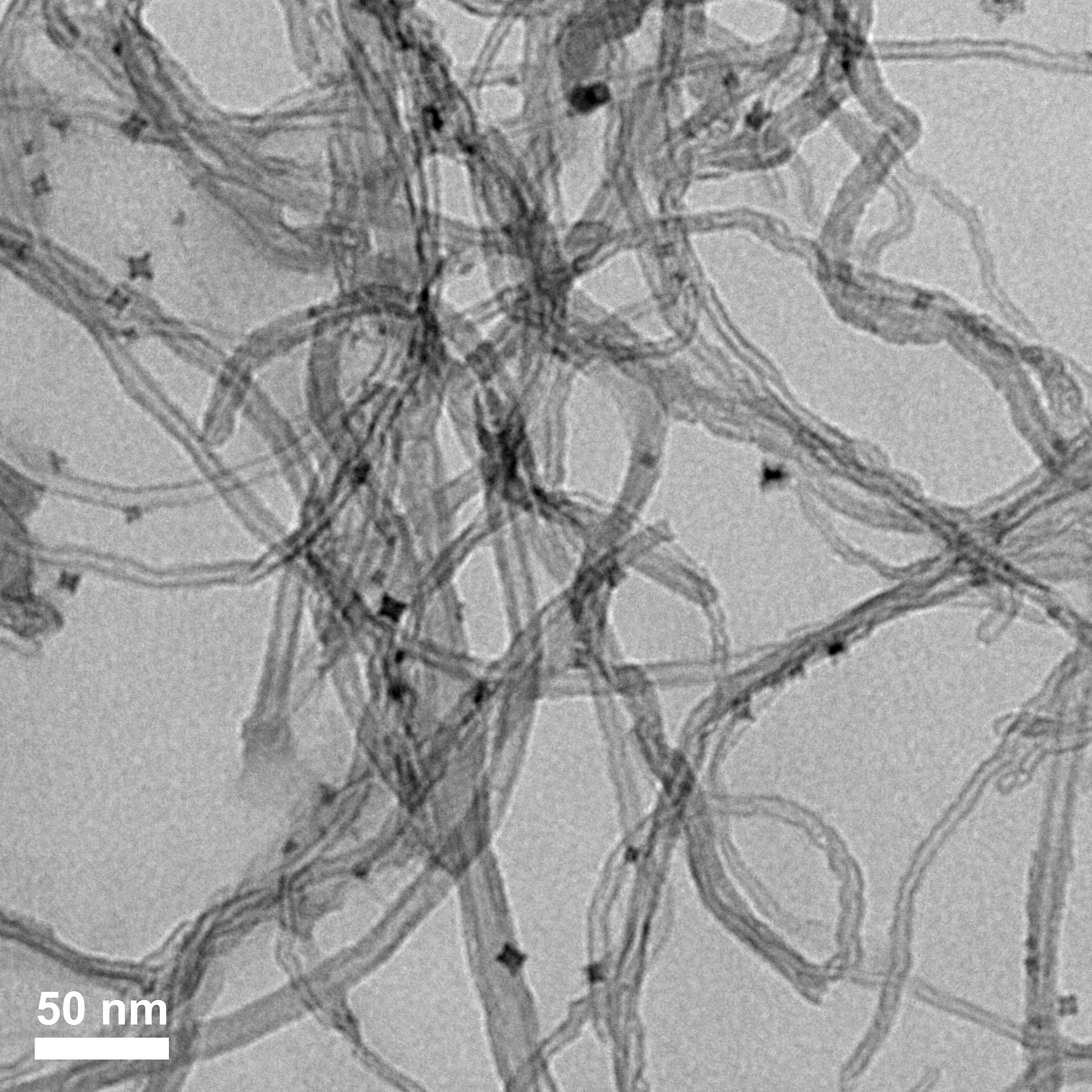
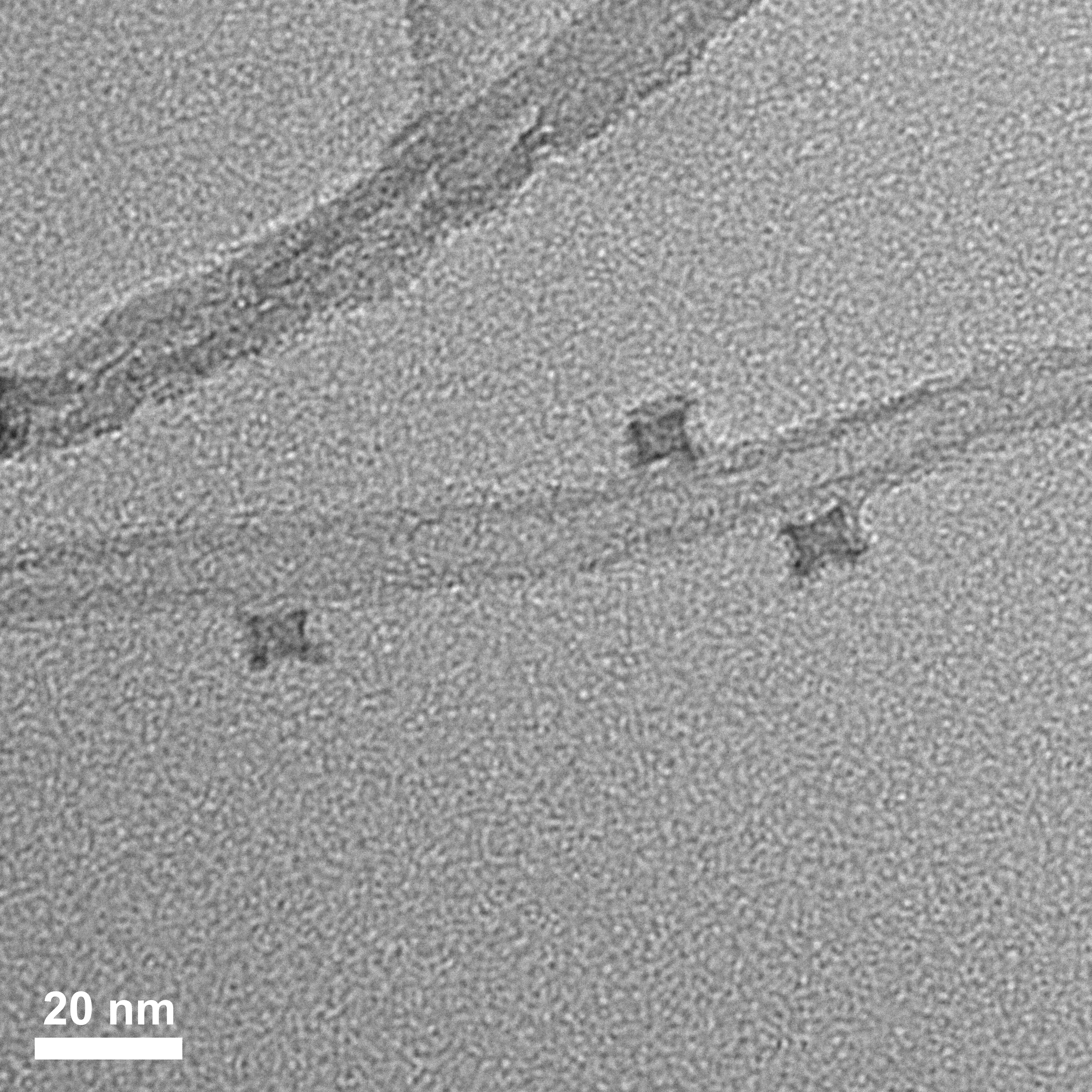
 TEM image of 10-nm cube-shaped metal oxide nanoparticles on carbon nanotubes. Objects appear dark against the bright background due to diffraction of the electrons emanating from the TEM's light source; the more diffraction occurs, the darker objects will appear. Credit: Jaeyoung Hong.One such researcher is Jaeyoung Hong, a first-year graduate student in materials science and engineering. Hong is using Beckman’s (S)TEM to image carbon nanotubes, cylindrical structures made of carbon atoms about one billionth of a meter
in diameter. Carbon nanotubes are known for their high electrical conductivity and mechanical properties, but Hong is interested in their function as a substrate for inorganic nanoparticles. The nanoparticles are perched on the nanotubes like birds
on a telephone wire. Like birds, their tendency is to aggregate; positioning them on a surface prevents such aggregation and loss of particles’ individual properties and its high surface area.
Acting primarily as a transmission electron microscope, the (S)TEM is instrumental in determining the size and positioning of nanoparticles on the telephone-wire nanotubes.
 Jaeyoung Hong“While high-resolution nanoparticle imaging is possible with a handful of machines, the TEM is built for it. With the SEM you can see the exterior, but with the (S)TEM you can see the internal structure – you can actually see through the material
and look at the atoms inside. For my research, I need this capability to see the array of the atoms at the surface of nanoparticles.
“For me, producing these images is proof that we can actually create composite nanomaterials; like how people say, ‘seeing is believing.’ It’s some of the most impressive, decisive data that you can produce,” Hong said.
To learn more about the Microscopy Suite, visit its web page: https://itg.beckman.illinois.edu/microscopy_suite
The (S)TEM, and other instruments in the Microscopy Suite, are available for use by all Illinois researchers and select visiting faculty. To request equipment training or use of the machines, please contact Microscopy Suite Manager Cate Wallace: ctopha2@illinois.edu
Beckman Institute’s scanning transmission electron microscope was purchased from TSS Microscopy, a microscope refurbishment and vending company based in Hillsboro, Oregon.
Beckman Institute for Advanced Science and Technology
