Article
Atomic Precision: There’s Still Plenty of Room at the Bottom
In Richard Feynman’s prescient 1959 speech “There’s Plenty of Room at the Bottom,” he conjectured that the digital atomic nature of matter presented vast untapped potential for information storage. The development of the scanning tunneling microscope (STM) in the early 1980’s at IBM Zurich, and ‘IBM,’ written with 35 Xenon atoms in 1990 by Don Eigler at IBM Almaden, ushered in the modern era of nanotechnology. Paralleling this, steady progress in semiconductor technology, following Moore’s Law, has led to commercial chip technology with 14 nanometer feature sizes; a distance spanned by about 35 silicon atoms.
The convergence of these parallel paths forms the basis of our research at Beckman, where we are exploring atomically precise fabrication on silicon surfaces. To this end, we have developed the ability to pattern silicon with single atom precision using a STM. This talk will show how we do this as well as the unexpected spin-off that has led to the use of deuterium in current chip production. We are now combining our ‘top-down’ atomic precision STM work with ‘bottom-up’ atomically precise structures. Specifically, carbon nanotubes and graphene nanoribbons are being actively considered as the core transistor structures for future chip technologies. We have developed methods to integrate and study these carbon-based systems with conventional semiconductors like silicon.
We have also developed a method to link carbon nanotubes for improved performance of composite materials, and we have invented a process for making STM probes that has been commercialized by Tiptek for semiconductor companies to use in probing their advanced chip technologies.
Speaker biography

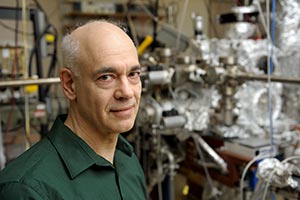
Joseph Lyding is the Robert C. MacClinchie Professor of Electrical and Computer Engineering at the University of Illinois at Urbana-Champaign. He received his Ph.D. in electrical engineering from Northwestern University in 1983. He joined the Illinois faculty to work with Nobel laureate John Bardeen on the 1D charge-density wave problem. During that time, he developed the first scanning tunneling microscope in the Midwestern United States, with which he developed the atomic resolution hydrogen resist process for patterning silicon surfaces. In these experiments, he also discovered the giant deuterium isotope effect that is now being used in large-scale chip production to reduce hot-carrier degradation in CMOS technology. Recently, he has developed a method to improve the performance of carbon nanotube transistors and he invented a technology for producing ultra-sharp hard-coated electrically conductive probes for scanned probe microscopy that has recently been commercialized. Lyding was selected as a UIUC University Scholar, and he is a Fellow of the APS, IEEE, AVS and AAAS. He received the 2012 IEEE Pioneer in Nanotechnology Award, the 2013 AVS Nanotechnology Recognition Award, the 2013 Research Excellence Award from the Nano/Bio Interface Center at the University of Pennsylvania, the 2014 AVS Prairie Chapter Award for Outstanding Research, and the 2014 Feynman Prize in Nanotechnology.
Beckman Institute for Advanced Science and Technology