Article
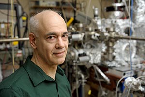
For his groundbreaking research, Lyding, a professor of electrical and computer engineering, recently was awarded the Foresight Institute Feynman Prize for experimental work. The Foresight Institute is a leading think tank and public interest organization focused on transformative future technologies.

According to a Foresight Institute announcement, “Lyding is a pioneer in the development of STM technology and particularly hydrogen depassivation lithography. While many other STM practitioners have used the tool to do atomic and molecular manipulation of atoms and molecules on surfaces, hydrogen depassivation lithography is a generic patterning technique using a resist that allows pattern transfer to enable many different types of structures and functionalization of surfaces, all while maintaining atomic resolution and precision.”
In other words, Lyding has been able to achieve atomic resolution patterning of hydrogen-terminated silicon surfaces with an ultrahigh vacuum scanning tunneling microscope.
“We do our work in an ultrahigh vacuum, which is important if you want to look at something that’s clean: you have to get rid of all contamination influences,” explained Lyding. “That would be 14 orders of magnitude lower pressure than the atmosphere. So it’s really a deep space kind of vacuum.”
Lyding says that chance played a part in the creation of his STM microscope.
“It was stunning. I was mowing my lawn, and the idea for the microscope just appeared in my brain,” said Lyding. “I think I kept mowing into my neighbor’s yard.”
Although Lyding claims that the STM, which uses conducting tips to scan a surface and a tunneling current to create images, is fairly easy to design, using it to examine and modify surfaces at the atomic level requires more than luck.
“The equipment was built from scratch, but these are fairly simple instruments in reality,” said Lyding. “How they work really depends on things like vibration sensitivity and thermal expansion of components. When you’re dealing with things that move relative to each other at the atomic scale, any kind of thing that influences that like vibration or thermal expansion wreaks havoc. So my design really solved that problem. It’s the one we still use and it has been adopted by many groups worldwide.”
Spinning Off
A spin-off of Lyding’s STM nanotechnology research was the discovery that deuterium can be used to dramatically reduce the wear and tear on integrated circuit transistors caused by energetic electrons. As a consequence, deuterium processing is now used in advanced chip production under license from the University of Illinois.
A recent development in Lyding’s group is a technique to improve the performance of carbon nanotube-based array transistors by linking the nanotubes together at their junctions. Current flow generates heat at these junctions, which can be used to drive a thermal metallization process that encases the junctions in metal, improving transistor performance by an order of magnitude.
This general technique also has great promise for improving the mechanical and thermal properties of carbon nanotube-based composite materials. Seed funding from the Beckman Institute enabled the NANOSTRONG project, which aims to strengthen carbon nanotube-based structural materials. While the new materials are lightweight and strong, they lack the intrinsic strength that is found in individual nanotubes because of how the materials are connected to one another, said Lyding. The NANOSTRONG project has also set the foundation for exploring dramatically improved thermal properties in composite materials.
P.O.E.T.S.
As part of the new Power Optimization for Electro-Thermal Systems (POETS) Center, Lyding is now translating this technology into the development of high-conductivity thermal routing conduits. Led by Andrew Alleyne, a professor of mechanical science and engineering at Illinois, POETS is an $18.5 million engineering research center that aims to pack more power into less space for electrical and mechanical systems. The center is funded by the National Science Foundation and is headquartered at the University of Illinois at Urbana-Champaign.
“If you want to remove heat from a hot object efficiently, you need a good thermal conductor,” said Lyding.
The process of connecting the carbon nanotubes allows for stronger and more powerful materials to be created, but understanding how the connection functions will enable better thermal conduits and stronger structural materials.
“That’s where the atomic resolution imaging comes in,” said Lyding.
Pinshane Huang, an assistant professor of materials science and engineering at Illinois, is working with Lyding, using an atomic resolution transmission electron microscope to look at the junctions and their atomic detail.
“Then we can start optimizing,” said Lyding. “We can start thinking, now that we understand how it works, we can understand how to optimize it, or, if we want to change it in some as yet unforeseen way, we know where the knobs are that we can turn and what they’re going to do.”
“All these things, the key ideas that have led to technology, these are all accidental, every one of them,” said Lyding. “Nothing was planned, it’s just all of a sudden ‘Ah, what if we tried this?’“
Although Lyding might claim to be lucky in his discoveries, it probably comes down to his ability to think about things differently than others.
“Any kind of idea like these in retrospect is obvious, it’s just why didn’t other people do it?” said Lyding.
Beckman Institute for Advanced Science and Technology